Complex Functional Materials
|
|
Selected Publications
|
Our information age traces back to wartime invention of methods to fabricate silicon and germanium crystals with defects lower than 1 part in 100, a threshold at which the intrinsic properties could then be applied. Today, complex materials (>2 elements with periodic atomic ordering) are at a similar inflection point. Improvement beyond 1 defect in 4 has proven challenging: energetic defects abound and many elements are not compatible with current low-defect growth techniques. My goal is to develop new pathways to complex material thin film systems with 99% atomic ordering in today’s “too-complex” materials.
My group and I have identified two major roadblocks associated with poor ordering, one intrinsic and one extrinsic in nature:
(1) Phase formation energies are intrinsic to specific material systems and specific atomic positions. A highly ordered complex material cannot form if the (formation) energy difference between a fully ordered and a disordered/site-swapped materials is less than, or even comparable to, the available energy in the region, especially during synthesis.
(2) High-energy effects during synthesis (extrinsic). The energy scale of incident material during deposition allows crystalline and site disorders to occur. If that energy scale is larger, site swapping is easily done and disordered material will occur. As such, even in a thermodynamically favorable system will be critical to synthesize the material while minimizing sources of energetic damage. Minimizing this damage to enable and study new materials is the fundamental basis, and competitive advantage, of my research.
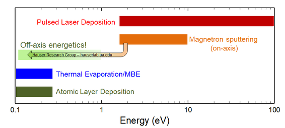
The above figure shows typical energies for various Physical Vapor Deposition methods. Molecular Beam Epitaxy (MBE) and Atomic Layer Deposition techniques can currently be tuned to provide the ~0.1 eV energetics required for complex materials, but cannot easily or reliably work with a large swath of elements (particularly, and crucially, many transition metals), grows films extremely slowly, and is relatively expensive. Pulsed laser deposition can be tuned to energies as low a few eV. Conventional on-axis magnetron sputtering can typically only reach 1-2 eV as well but is fast, reasonable cost, and has the widest elemental range of any technique.
Heusler alloys are an excellent testbed for new growth techniques, since atomic ordering is currently stalled at 70-80%, far too low to see intrinsic properties and make application-quality films. Part of this is elemental choice, but 1-2 eV of energetics will cause site disorder in most complex materials. A way forward is off-axis geometry sputtering, with which I demonstrated 99% Cr/Re ordering in a four-element double perovskite oxide (PRB 85, 161201, 2012). Composition control is difficult in composite-target off-axis sputtering due to variations in scattering and ejection dispersion of different elements, growth-to-growth changes as the target shape changes, and position dependent flux variation. Solving this challenge required employing beam shaping, shuttering and flux control methods used in MBE, with a combinatorial sputtering approach with rapid substrate rotation (2-3 times faster than typical rotation rates). The shutter shape results in uniform, beam-like flux behavior. This, combined with the heavy usage of MBE-inspired control techniques (and some playful banter with MBE-using colleagues), resulted in our name for the method: Sputter Beam Epitaxy.
Heusler alloys are an excellent testbed for new growth techniques, since atomic ordering is currently stalled at 70-80%, far too low to see intrinsic properties and make application-quality films. Part of this is elemental choice, but 1-2 eV of energetics will cause site disorder in most complex materials. A way forward is off-axis geometry sputtering, with which I demonstrated 99% Cr/Re ordering in a four-element double perovskite oxide (PRB 85, 161201, 2012). Composition control is difficult in composite-target off-axis sputtering due to variations in scattering and ejection dispersion of different elements, growth-to-growth changes as the target shape changes, and position dependent flux variation. Solving this challenge required employing beam shaping, shuttering and flux control methods used in MBE, with a combinatorial sputtering approach with rapid substrate rotation (2-3 times faster than typical rotation rates). The shutter shape results in uniform, beam-like flux behavior. This, combined with the heavy usage of MBE-inspired control techniques (and some playful banter with MBE-using colleagues), resulted in our name for the method: Sputter Beam Epitaxy.
